- Speeds time-to-market with flexible software options, simplified system integration and synchronization, and application-specific measurement capabilities
- Scalable, compact solution that gives digital development engineers up to 20 source measure unit channels in a 1U form factor
- Reduces costs by integrating pulser and digitizer functions with conventional source and measure functions for an all-in-one solution
Keysight Technologies, Inc. (NYSE: KEYS) introduces the PZ2100 Series High-Channel Density Precision Source Measure Unit (SMU) Solution, a new SMU solution giving digital development engineers 20 precision SMU channels within a 1U rack space to speed the characterization of integrated circuit (IC) designs.
This press release features multimedia. View the full release here: https://www.businesswire.com/news/home/20230711344613/en/

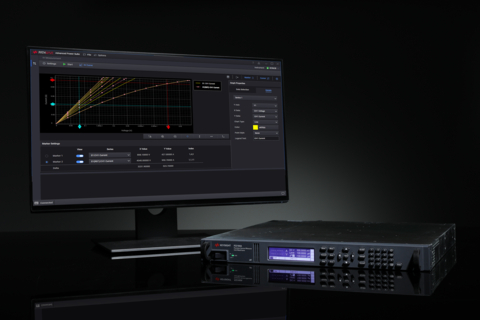
The Keysight PZ2100 Series High-Channel Density Precision Source Measure Unit (SMU) Solution provides digital development engineers 20 precision SMU channels within a 1U rack space to speed the characterization of integrated circuit designs. (Photo: Business Wire)
While innovation cycles are shortening and digital standards are evolving, designing a semiconductor component or device and delivering it to market remains a time-intensive, technical process. Digital development engineers must connect and test multiple ports on a single device-under-test (DUT) throughout the design cycle to troubleshoot and characterize the performance of the IC. Without high-density, automated characterization solutions, engineers risk slowing their delivery timelines as they validate with complex, multiport designs using complicated and low-density test setups.
Keysight’s PZ2100 Series SMU addresses this risk by giving design engineers a high-density SMU solution that is scalable to 20 SMU channels in a compact 1U rack configuration. The solution also speeds time-to-market with flexible software options, simplified system integration and synchronization, and application-specific measurement capabilities, allowing them to focus more time on characterization and less on synchronization.
The PZ2100 Series SMU delivers the following benefits:
- Single-box solution – Saves time by simplifying channel stacking and synchronization to remove integration and coding complexity. The user-friendly GUI accelerates test prototyping, debugging, and troubleshooting while the PathWave IV Curve Measurement software enables quick measurements and synchronization without programming.
- Scalable, compact, and flexible – Saves rack space by offering up to 20 SMU channels in a valuable 1U full-width form factor that does not require cooling spacers when stacked. Available in five SMU module options that are configurable and upgradeable.
- All-in-one SMU module – Reduces cost by integrating pulser and digitizer functions with conventional SMU functions, such as precise DC voltage and current sourcing and measuring to meet emerging requirements without additional instruments.
Toshio Kimura, General Manager for Furukawa Electric's Next Generation Components Development Department, Next Generation Photonics Business Innovation Project Team, said: “By embedding Keysight's PZ2100 High-Channel Density Precision SMU into our test system, it increases our test throughput for developing and mass-producing optical components for broadband, long-distance transmission. In addition, it helps us reduce our test system footprint with up to 20 channels of SMUs installed in a 1U rack space. This flexible, scalable, and modular solution can also accommodate future test needs, helping to reduce overall test costs. Keysight's extensive product portfolio and metrology expertise drives our business success, allowing us to continue to lead the optical component industry.”
Carol Leh, Vice President and General Manager for Keysight's Electronic Industrial Solutions Group's Center of Excellence, said: "With options that scale up to 20 SMU channels, the PZ2100 Series offers five times more channel density than equivalent SMUs, making it the highest channel density SMU in a 1U form factor in the market. Combine this with the PathWave IV Curve software for quick, programming-free IV measurements, and you have a solution that allows you to focus more of your time on actual characterization and less time on synchronization and system bring-up."
Resources
- Keysight PZ2100 Series High-Channel Density Precision Source Measure Unit
- Keysight University PZ2100 SMU Learning Resources
About Keysight Technologies
At Keysight (NYSE: KEYS), we inspire and empower innovators to bring world-changing technologies to life. As an S&P 500 company, we’re delivering market-leading design, emulation, and test solutions to help engineers develop and deploy faster, with less risk, throughout the entire product lifecycle. We’re a global innovation partner enabling customers in communications, industrial automation, aerospace and defense, automotive, semiconductor, and general electronics markets to accelerate innovation to connect and secure the world. Learn more at Keysight Newsroom and www.keysight.com.
View source version on businesswire.com: https://www.businesswire.com/news/home/20230711344613/en/
Contacts
Geri Lynne LaCombe
Americas/Europe
+1 303 662 4748
geri_lacombe@keysight.com
Fusako Dohi
Asia
+81 42 660-2162
fusako_dohi@keysight.com


